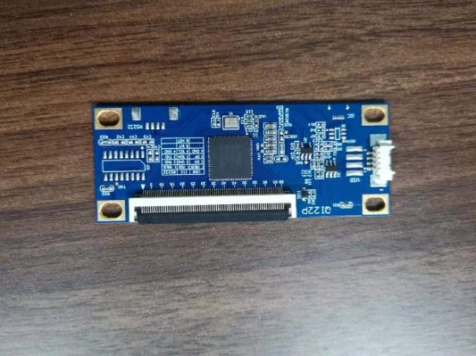
Concept and function of PCB processing
PCB processing and proofing refers to making a sample for customers and manufacturers to inspect, test and verify themselves before mass production of circuit boards.
This process usually includes designing schematic diagram, making PCB layout, printing circuit board, drilling and mounting components, and welding.
The purpose of PCB processing and proofing is to ensure that the circuit board functions normally, meets the customer's requirements, can be mass-produced,
and reduce the later production cost and time. Therefore, it plays a very important role in the development of electronic products.
The process of PCB processing and proofingThe process of PCB processing and proofing includes designing schematic diagram and making PCB layout, printed circuit board,
drilling and mounting components, welding and other steps. These steps will be described in detail below.
Design schematic diagram and make PCB layout diagramFirst of all, we need to design a schematic diagram according to customer needs and product functional requirements.
Schematic diagram is a graphical representation of circuit principle, which can clearly show the relationship and connection mode between components in the circuit.
After the schematic design is completed, it needs to be converted into PCB layout. PCB layout refers to arranging circuit patterns on PCB according to certain rules, and determining
the position and connection mode of each component. In general, PCB layout should consider the following factors:
1, the size and shape of the circuit board
2, the number and type of components
3. Connection mode and layout between components
4. Heat dissipation and arrangement of the circuit board
PCB Printing
After the PCB layout is completed, the circuit pattern needs to be printed on the circuit board by chemical method. This process is called PCB printing, and the printing process includes the following steps:
1. Select the appropriate circuit board material and thickness;
2, coating a layer of copper foil on the surface of the circuit board, and then sticking a photosensitive film on it;
3. The PCB layout is irradiated onto the photosensitive film on the surface of the circuit board through the projector and other equipment, so that only the sensitivity of the circuit pattern part is changed;
4, putting the circuit board into an etching tank for chemical etching to remove unnecessary copper foil;
5. Clean the etched circuit board to remove the photosensitive film and other dirt.